
Power delivery systems in modern handheld electronics require clean conversion between battery discharge voltages and fixed IC logic rails. Linear regulators offer low noise but waste excessive power as heat whenever a significant differential exists between input and output voltage. Switching regulators solve this thermal problem, but choosing between buck, boost, or buck-boost topologies depends directly on your source voltage behavior under load.
Inductor Sizing and Switching Loss Tradeoffs
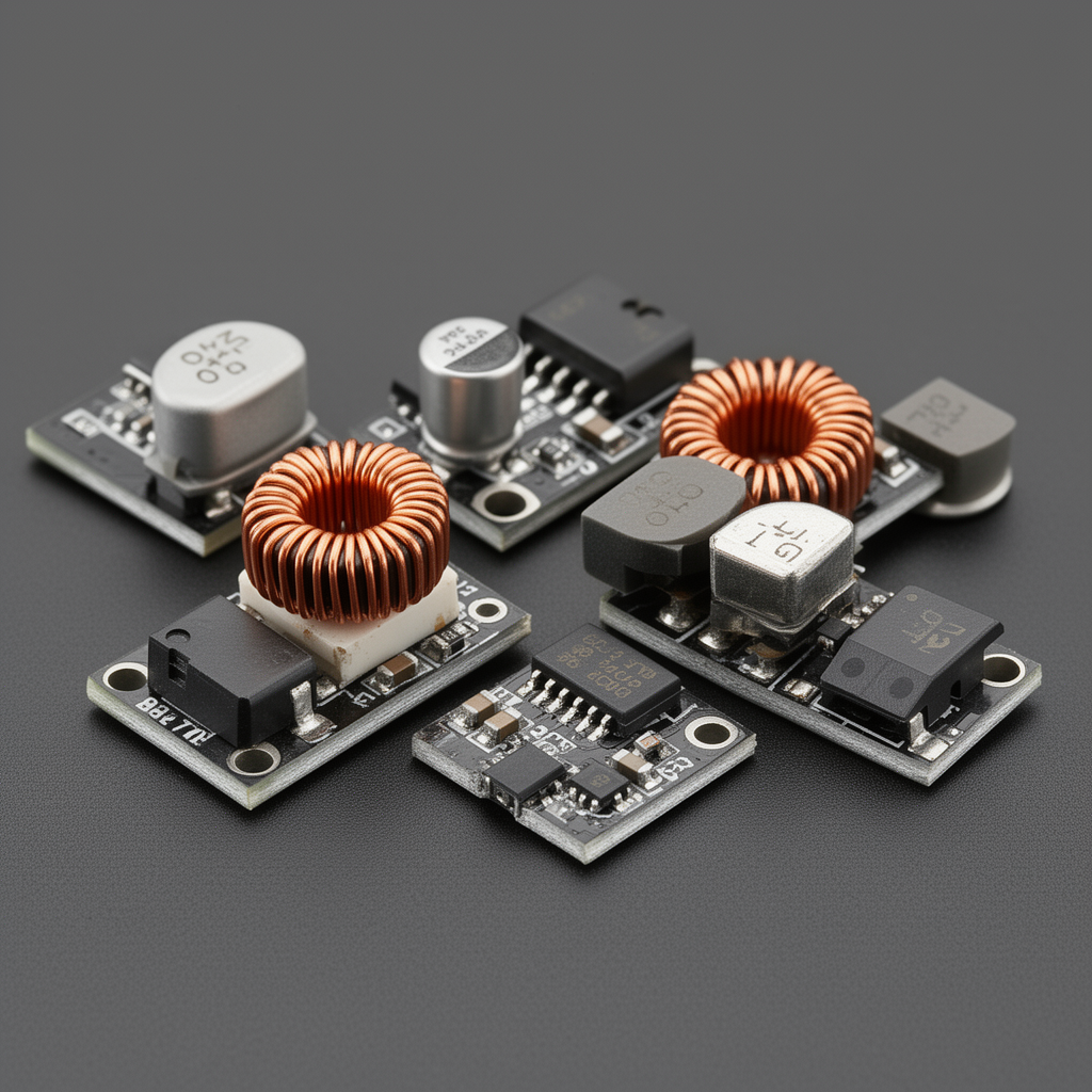
Buck regulators step higher voltages down by rapidly toggling internal MOSFETs, smoothing the pulsating current through a power inductor and storage capacitor. Boost regulators flip this configuration to step lower voltages up, requiring inductors capable of handling higher peak saturation currents. Higher switching frequencies allow engineers to specify physically smaller surface-mount inductors, but this increases switching gate drive losses across the integrated switching silicon.
Thermal Dissipation and Power Delivery Efficiency
Under heavy load conditions exceeding two amperes, synchronous buck converters with integrated low-resistance switches achieve conversion efficiencies above ninety percent. Non-synchronous designs using external Schottky diodes suffer higher forward voltage drops, creating thermal hotspots on dense board layouts. When operating from single-cell lithium chemistry where input voltage swings above and below a target three point three volt rail, custom buck-boost topologies ensure stable power delivery without thermal throttling.
Practical Guidelines for Power System Selection
For battery-powered devices with tight space constraints, choose integrated synchronous buck ICs like the TPS62130 to keep board temperatures cool and extend runtime. When boosting low single-cell input sources up to standard five volt USB logic rails, calculate inductor saturation limits carefully to prevent voltage ripple under sudden load spikes.